300mm Wafer Notch Size
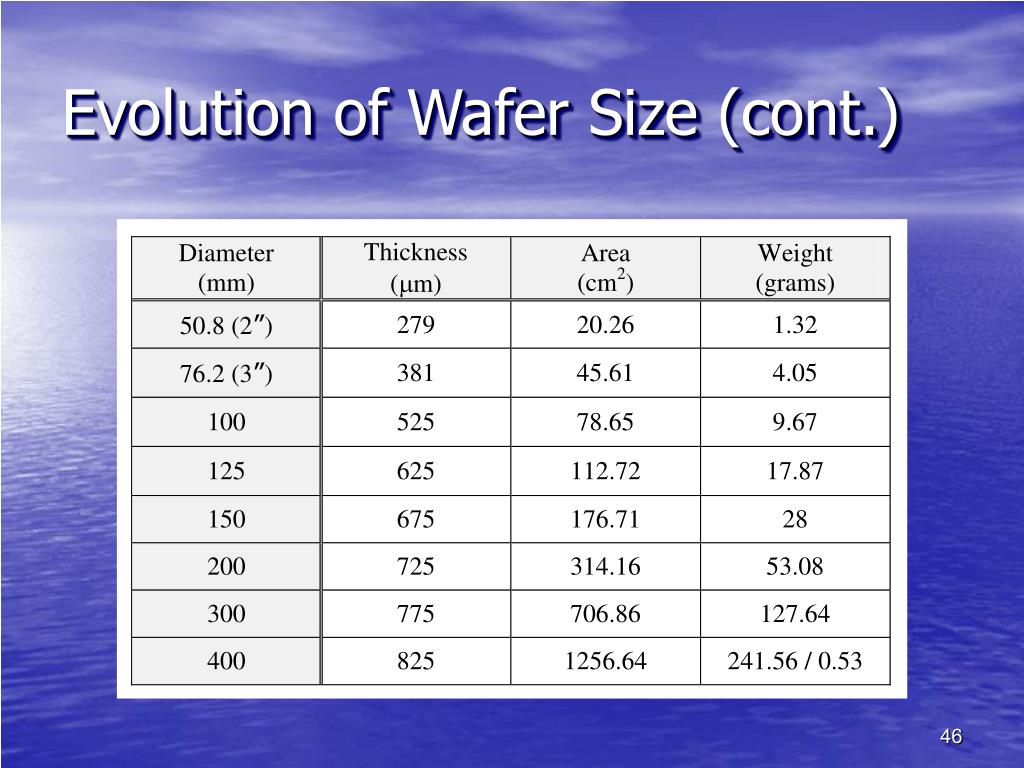
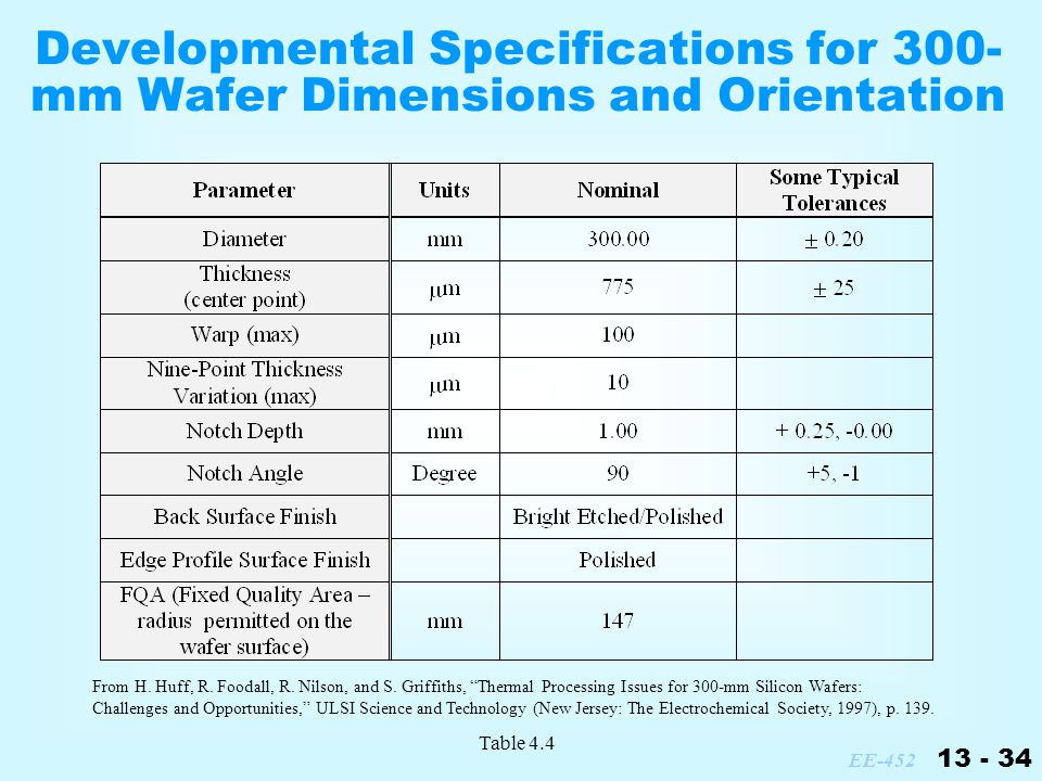
 Wafer Dimensions And Parameters
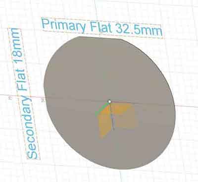
 Glass Wafer Semi Standards Glass Wafer Notch Semi Flats
Http Www2 Ensc Sfu Ca Glennc E495 E495l2o Pdf
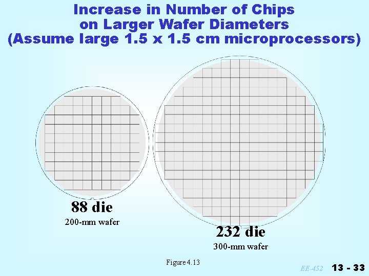
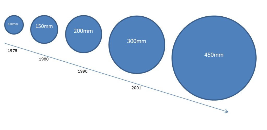 Does Size Matter Understanding Wafer Size
 Watom Wafer Edge Profil Measurement System Eltech Group Solutions Consulting
Https Sydor Com Wp Content Uploads 2019 06 Semi Wafer Flat M1 0302 Specifications Pdf
 Mock Wafer 12 300mm Notched 6061 T 6 Anodized Aluminum Alloy Hard Clear
 This Is What 450mm Wafers Look Like
 The Wafer Waferfabrication Semiconductor Technology From A To Z Halbleiter Org
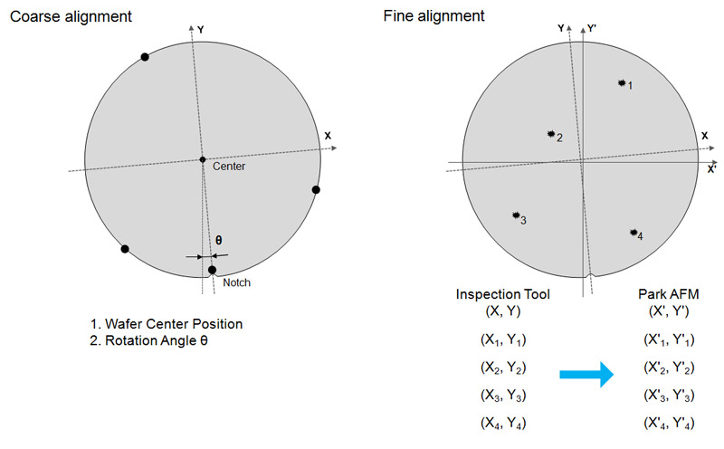 Automatic Defect Review Adr Of 300mm Bare Wafers With Automated Afm
Http Www Ensc Sfu Ca Glennc E495 E495l2j Pdf
 Silicon Wafer An Overview Sciencedirect Topics
 Wafermap Convert Glossary Of Terms
 Manufacture Of Mos Devices Springerlink
 Wafer Electronics Wikipedia
Https Nanopdf Com Download Draft 450mm Mechanical Wafer Spec Rev 14 Pdf
Http Www Ensc Sfu Ca Glennc E495 E495l2j Pdf
Https Www Microchemicals Com Technical Information Silicon Wafer Production Specification Pdf

 Wafer Electronics Wikiwand
 Wafers And Transistors Springerlink
Http Downloads Semi Org Web Wstdsbal Nsf 0 Eb834168722f4f9188257ea00028c2e2 File 5890 Pdf
1
What Is It Like To Work In A Microchip Factory Quora
 Why Do Silicon Wafers Have Flats Cut Out Of The Wafer Edge
Https Www Osapublishing Org Viewmedia Cfm Seq 0 Uri Osac 2 7 2098
 Wafer Electronics Wikiwand
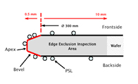 Psl Particle Wafer Standards Edge Contamination Standards Vlsi Particle Standards

 Studying Post Etching Silicon Crystal Defects On 300mm Wafer By Automatic Defect Review Afm
 The 300 Mm Silicon Wafer A Cost And Technology Challenge Sciencedirect
 Slip Band Distribution In Rapid Thermally Annealed Silicon Wafers Journal Of Applied Physics Vol 111 No 9
Https Www Electrochem Org Dl Interface Wtr Wtr06 Wtr06 P28 31 Pdf
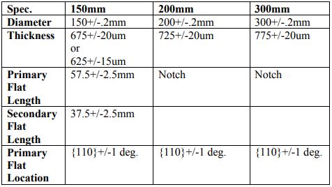
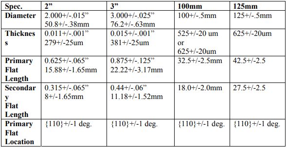
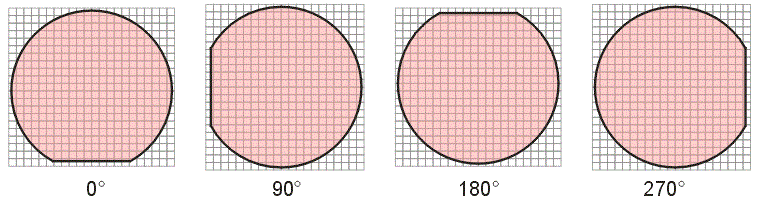
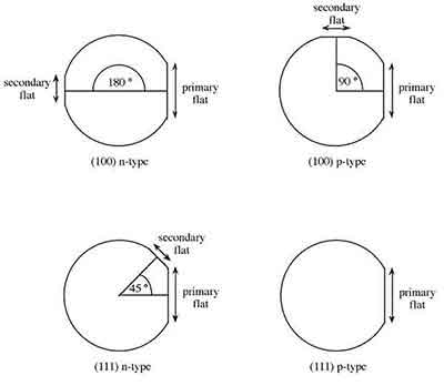
 Flats
Flats
 Wafermap Convert Glossary Of Terms
 Silicon Crystal Structure And Growth Plummer Chapter 3 Ppt Video Online Download
 Wafer Electronics Wikipedia
 Ultron Systems Inc Grip Rings Film Frames Shippers Magazines


 Technology Globalwafers
 Glass Wafers Of Borosilicate Af32 D263 Bk7 Quartz Glass
 100 Orientation Silicon Wafers With Notches Flat Cuts
.jpg) Post Etching Silicon Crystal Defects On A 300 Mm Wafer
Post Etching Silicon Crystal Defects On A 300 Mm Wafer
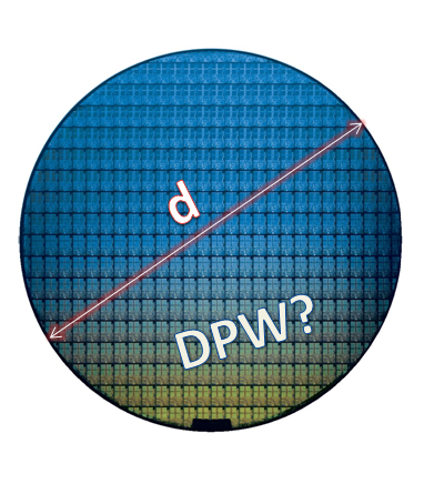 Die Per Wafer Free Calculator
 What Are Silicon Wafers Where Are They Used Article

1
Http Www Ensc Sfu Ca Glennc E495 E495l2j Pdf
 Technology Globalwafers
Https Moodle Fel Cvut Cz Mod Resource View Php Id 59606
 Wafer Preparation Mohammad Pourmand Course Lecturer Dr Jafari Panah Ppt Download
 Pdf Die Singulation Technologies For Advanced Packaging A Critical Review
 Engineering Wafer Electronics Handwiki
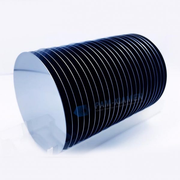
 300mm P B 1 0 0 1 25 Ohm Cm 775 25µm Prime Silicon Wafer Dsp One Semi Notch Ttv
 Silicon Crystal Pulling
Given That The Wafer Size Is Crucial For Production Yields If The Semiconductor Industry Switches To Other Materials E G Gan Or Sic Is It Possible To Manufacture Wafers Of A Size Comparable
 The Wafer Waferfabrication Semiconductor Technology From A To Z Halbleiter Org
 20nm Node Broken For Gpus
Http Www Prostek Com Ch Data Semiconductor 20wafer 20edge 20analysis Pdf
 Silicon Wafers Preparation And Properties Sciencedirect
 High Throughput Automatic Defect Review For 300mm Blank Wafers With Atomic Force Microscope
Https Nptel Ac In Content Storage2 Courses 113106062 Lec21 Pdf
 Wafermap Convert Glossary Of Terms
 What Are Silicon Wafers Where Are They Used Article
 Kocos Eltech Group Solutions Consulting
Ppt Wafer Manufacturing Powerpoint Presentation Free Download Id 4841268
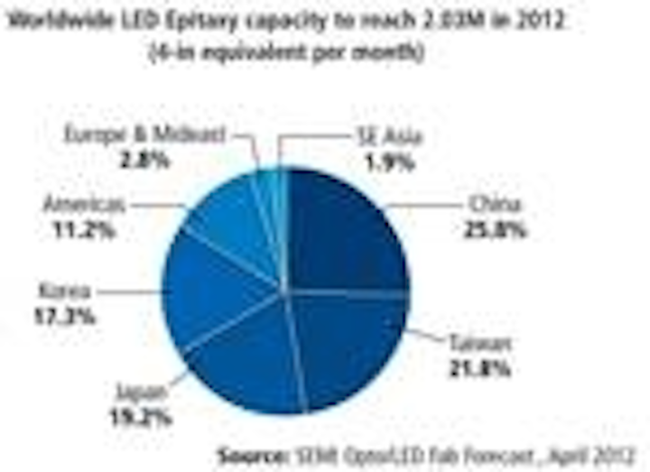 Semiconductor Industry Moves Toward Automated Led Production On 6 Inch Wafers Magazine Leds Magazine
 Challenges And Solutions For Silicon Wafer Bevel Defects During 3d Nand Flash Manufacturing Coventor
 China Lg Lf350 Cumin Spice Powder Packing Machine Factory On Global Sources Spice Powder Packing Machine Chili Powder Packing Machine Baking Powder Packing Machine

 Ra321 C0c Bw Rorze
1
 300mm Silicon Wet Or Dry Thermal Oxide Dioxide Wafers Si Sio2 Powerway Wafer
 Elimination Of Strength Degrading Effects Caused By Surface Microdefect A Prevention Achieved By Silicon Nanotexturing To Avoid Catastrophic Brittle Fracture Scientific Reports
Https Community Jmp Com Kvoqx44227 Attachments Kvoqx44227 Discovery 2016 Content 63 1 Jmp 20discovery 202016 20 20all 20wafer 20maps 20are 20wrong Pdf
 A Larger Wafer Diameter Enables Producing More Semiconductor Devices From A Single Wafer Https Www Waferworld Com Semiconductor Wafer Solutions
 Apple A13 Beyond How Transistor Count And Costs Will Go Up
Http Www Prostek Com Ch Data Semiconductor 20wafer 20edge 20analysis Pdf
Https Ieeexplore Ieee Org Iel5 5 4357935 06178756 Pdf
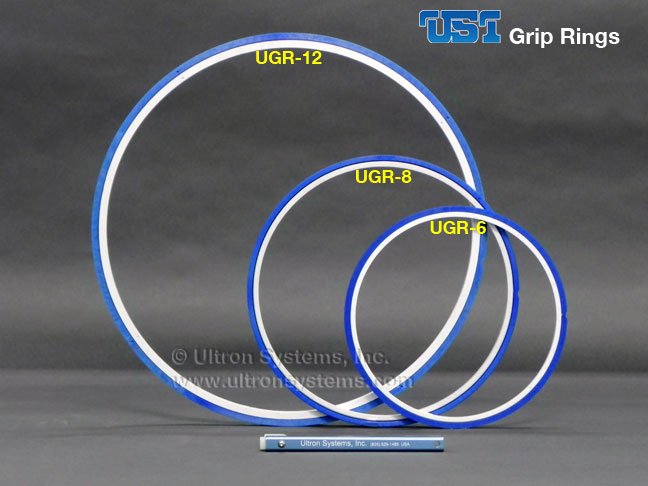 Ultron Systems Inc Grip Rings Film Frames Shippers Magazines
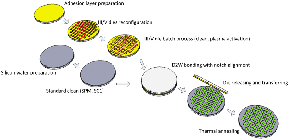 Frontiers High Throughput Multiple Dies To Wafer Bonding Technology And Iii V On Si Hybrid Lasers For Heterogeneous Integration Of Optoelectronic Integrated Circuits Materials
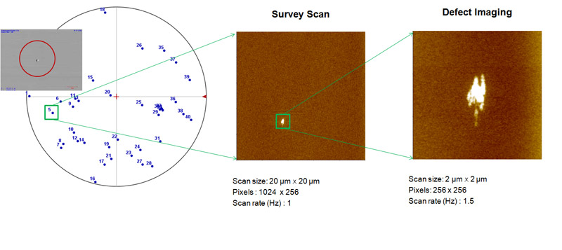 Automatic Defect Review Adr Of 300mm Bare Wafers With Automated Afm
 Silicon Substrates For Semiconductor Manufacturing Mcgraw Hill Education Access Engineering
 6 1 2 Silicon Crystal Growth
Https Www Mdpi Com 2079 9292 7 3 39 Pdf Vor
 Pdf Alignment Technology For Backside Integration
Http Www Ensc Sfu Ca Glennc E495 E495l2j Pdf
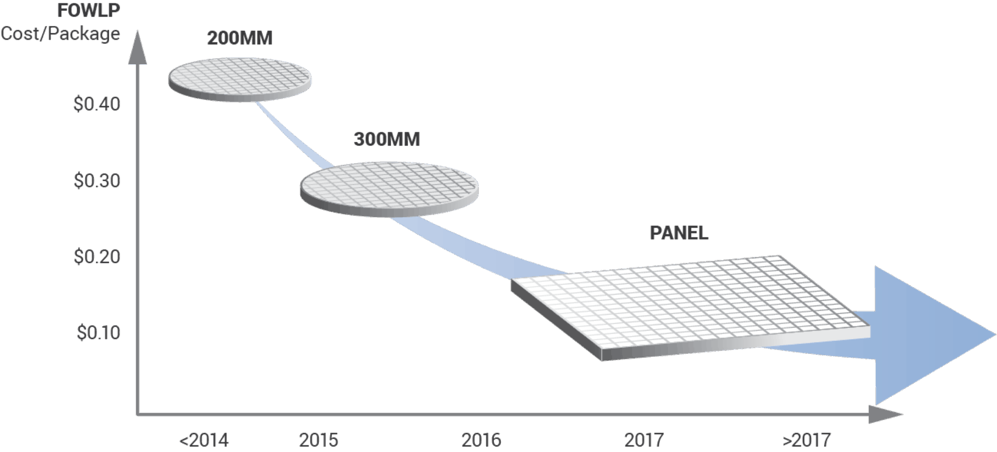 Lithography Challenges For Panel Level Packaging Onto Innovation
Https Www Kobelco Co Jp English Ktr Pdf Ktr 34 059 064 Pdf
 Silicon Crystal Structure And Growth Plummer Chapter 3
Https Www Electrochem Org Dl Interface Wtr Wtr06 Wtr06 P28 31 Pdf
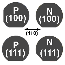
 What Is The Orientation Of Silicon Wafer 100 111 110
 Application Of Deterministic Resampling Particle Filter To Fatigue Prognosis Jve Journals
 Die Singulation Technologies For Advanced Packaging A Critical Review Journal Of Vacuum Science Technology B Vol 30 No 4
 300mm Bare Silicon Wafers 12 Inch Prime Grade N Type Or P Type With Orientation 100 111
1
 Silicon Crystal Pulling
2
 Float Zone Wafers Waferpro
 Wafer Pre Aligner System Based On Vision Information Processing Scialert Responsive Version